Authored by: Tom Cassidy and Sean Kelly


The following analysis and write up were performed by Nine Dot Connects reviewing a DDR3 layout in which the option for pin swapping was being considered. This is one of the many examples of the services provided to our customers.
Because signal integrity is so important to the operation of high-speed DDR3 design, and because the manufacturers of DDR3 devices are aware of the difficulties involved in high-speed impedance controlled PCB layout, they provided the flexibility of bit swapping within byte lanes to facilitate clean layout and good signal integrity. In particular, bit swapping allows the traces to be routed without needing to change layers. This greatly improves the signal integrity and thus the higher likelihood of producing a working design.
Bit swapping within DDR3 byte lanes is an accepted industry practice. The following is an excerpt from the Xilinx UG9333 Zynq-7000 PCB Design Guide, page 66:
https://www.xilinx.com/support/documentation/user_guides/ug933-Zynq-7000-PCB.pdf
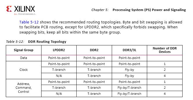
As the description of table 5-2 expresses, Xilinx specifically allows the use of both bit swapping and byte swapping. All bit swapping must be done within the same byte groups, and all byte groups (DQ, DQS, and DM) must be swapped as a whole.
It should be noted that bit swapping within the ACC (Address, Clock, and Control) group is not allowed.
Additional Information:
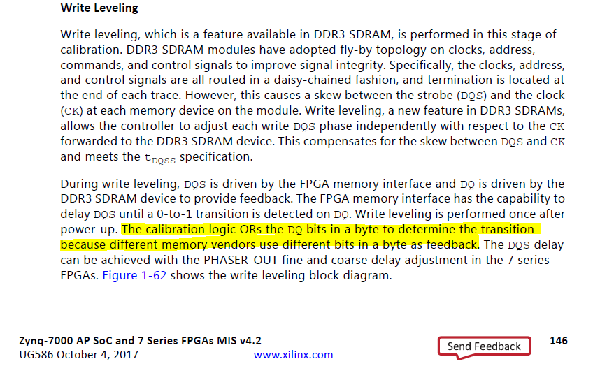
The JEDEC standard JESD79-3 states that a DDR3 memory device must either provide write-leveling feedback on all data pins or on the least significant bit (LSB) of the byte lane. If only one bit is used then all of the other bits must be set to 0.
NOTE: This JEDEC standard is referring to the memory devices themselves, not the memory controller. This often causes confusion, as one might read it as saying that the LSB must be wired one-to-one between memory device and controller. This is not the case.
Since there is not much consistency among memory vendors as to which feedback style used, most memory controllers perform a logic ‘OR’ on all of the bits in the data byte. This allows the memory controller to detect the feedback bit on any of the bits within the byte, thus supporting a full bit swapping within the byte lane.
From the Xilinx UG586 Zynq-7000 Series Memory Interface Solutions document:
https://www.xilinx.com/support/documentation/ip_documentation/mig_7series/v4_2/ug586_7Series_MIS.pdf