Preface: Mark Saunders is currently a senior at the Rochester Institute of Technology. He is one of the few undergraduate students with a working knowledge of PCB design. Although his focus is firmware, he has used Altium Designer for several personal and class projects.
I met Mark and his family through my daughter’s attendance at the same grade school. While in high school, he obtained a student license for Altium Designer with my assistance. Mark and I have kept in contact throughout the years.
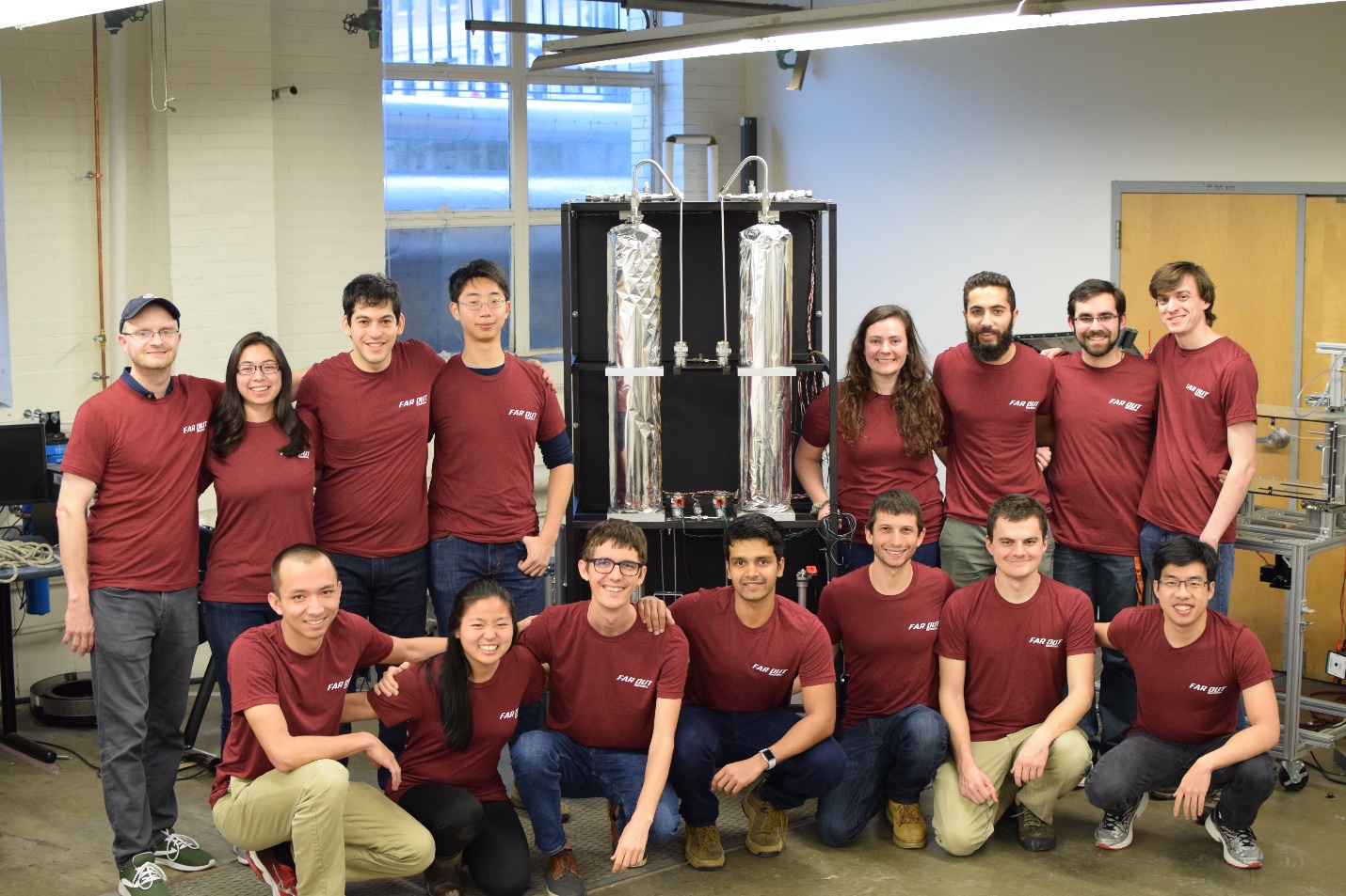
The Far Out Rocket Team. Mark Saunders is in the back row, second from the right.
Mark’s intern experience includes SpaceX where he met several other sharp individuals from various North American colleges and universities in different engineering disciplines. These interns decided to create the Far Out Rocketry team for the FAR-MARS launch contest. This is no easy feat since the team members are geographically separated. Mark’s role is a custom flight computer board design.
The adventure began at 9:00 PM PST on March 12th. In true engineering college fashion, Mark was up at midnight (EST) burning the candle at both ends. He called me, seeking guidance regarding a power short on his flight computer board. Three four-layer boards were made, one was populated. Power shorts were discovered on each board!
The problem with power shorts is they can be very difficult to track down. For the next hour, we discussed the issue and used GoToMeeting to look at the PCB layout together. There were no glaring violations, though I did think it was unusual that copper clearances were 5 mils. This tends to be at the cutting edge of price-sensitive fabricators. I asked about the fabricator but did not probe deep enough. This later became apparent.
What’s one to do? One suggestion that came from the rocket team was to crank up the voltage and see if there were any hot spots. Unfortunately, Mark did not have temperature sensing equipment available. He had a diamond bandsaw available at the time, so I suggested a binary search to cut the board down to where he could isolate the short through a diode check.
After the call was completed, my wife (also an engineer in the field of ICs) suggested there may be more than one power short. Sure enough, the next day Mark sent the picture below, confirming my wife’s suspicion:
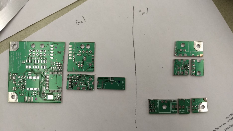
In further e-mail communications, Mark had discovered that the other board not only had similar shorts but also additional shorts. This made it clear that it was a fabrication issue.
In further discussions, I learned this fabricator had a student sponsorship program. If the layer stackup matches and panel real estate is available, the idea is to piggyback the student’s design onto a panel being run for a customer. These panels are usually 24″ X 18″, with approximately 1 inch of the panel edge being kept cleared for mounting equipment. Mark’s design was more than likely placed on the periphery of the panel. The center of the panel real estate is reserved for the company paying the standard rate for the fabrication.
Having a board fabricated on the periphery can be an issue due to possible misregistration between layers. The center is least impacted by such issues but misregistration nearing the edges can be more pronounced.

The secret of most fabricators is a customer’s design will be reviewed and modified by a CAM technician. They will clean up potential copper issues to ensure higher yield. However, one needs to understand that the customer’s design documentation and the fabricator’s documentation when the product is finished are not the same. This is why boards that work with a prototyping fabricator may not work with a fabricator in the business of “as is” mass production. Most fabricators will NOT disclose their work done on the board and most customers do not know their designs were modified.
While CAM service is provided to commercial customers, it is not likely provided to student projects. Also, Mark used the ruleset from the fabricator allowing 5 mils copper clearance. This clearance may have worked if a CAM technician cleaned up the board and the board was being placed in the center of the panel. In the redesign, Mark made the clearances more robust at 10 mils. The fabricator was very accommodating, allowing Mark another run of the board, this time with success.
There were lessons learned that go beyond an EDA tool. In the end, PCB designers must not only know the tools they are using to design the board but the fabrication process as well.
———————-
We at Nine Dot Connects understand that these are good lessons to learn in an undergraduate environment. However, they are not fun to learn in a work environment, where budget constraints and market windows (and career advancement) are on the line. That is why we created the PCB Foundations training. This three-day course is designed to walk you through the entire design process, conception through production, helping you become aware of the little things that make a big difference when manufacturing a board.
Authored by Paul Taubman