![]() Recently, Nine Dot Connects, a printed circuit board centric organization, became the national VAR for SOLIDWORKS PCB. With that came the opportunity to explore the mechanical side of design in our effort to better understand and prepare for the future of mechatronic design. Like the old saying, ‘Can’t see the forest for the trees’, this insight into the mechanical domain gave us the opportunity to step back and see the electrical design flow from afar. It became apparent when compared to mechanical libraries, the PCB library structure is complicated by several factors, some by the very nature of electrical design, and others are self-inflicted by the PCB industry.
Recently, Nine Dot Connects, a printed circuit board centric organization, became the national VAR for SOLIDWORKS PCB. With that came the opportunity to explore the mechanical side of design in our effort to better understand and prepare for the future of mechatronic design. Like the old saying, ‘Can’t see the forest for the trees’, this insight into the mechanical domain gave us the opportunity to step back and see the electrical design flow from afar. It became apparent when compared to mechanical libraries, the PCB library structure is complicated by several factors, some by the very nature of electrical design, and others are self-inflicted by the PCB industry.
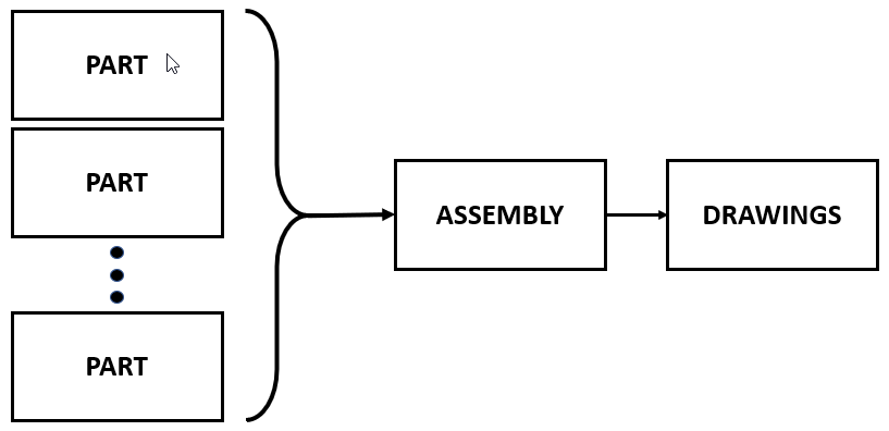
The Design Process
The mechanical design process is linear. One creates the part, and by creating the part, also creates a library component. That part is combined with others to form an assembly. By creating an assembly of parts, MCAD tools can quickly pull together the drawing (a.k.a. the blueprint) for manufacturing. It is a linear design process that builds upon itself.
In the PCB design domain, however, there are four editors. We need to have two representations of the electronic component; the symbol for the schematic and the footprint for the PCB layout. Once we create the symbol or footprint, we must place them onto the schematic editor and layout editor, respectively.
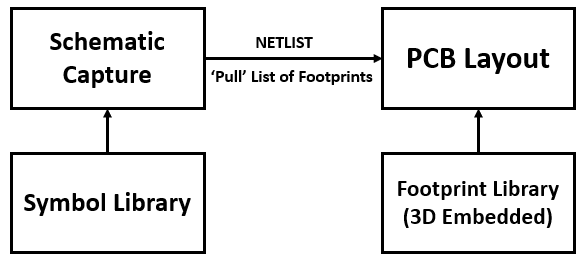
We create a schematic with all the symbols and wire them together. Upon completion, we push a netlist over. In tools like SOLIDWORKS PCB, if we’ve properly created and linked footprints to the symbol, we get a pile of footprints (in no particular order) adjacent to PCB, along with connection lines (generally referred to as the rat’s nest) to provide some guidance about connectivity between components. Then the process of placing the components and routing commences. In short, we create two drawings from scratch! PCB designers do not get the benefit of building the PCB directly off of the schematic. The schematic is conceptual and dimensionless; the PCB layout is physical.
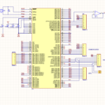
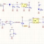
Three schematics – completed schematic design
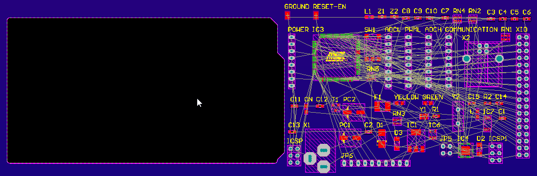
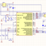
Information extracted from the schematics (minus the board shape)
Lack of a Universal Library Format in ECAD
MCAD tools like SOLIDWORKS CAD make use of the STEP format. While no MCAD tool uses this as its default format, it can import and export STEP. This allows companies and component distributors to provide graphical representations of their products. This is a monumental time saving to the mechanical designer. Even electrical designers using SOLIDWORKS PCB who have little mechanical skills or access to such skills benefit from 3D components being widely available.
Yet, nothing like this exists for ECAD. The EDA companies are so protective of their formats and market share, they make no effort to create an equivalent format to STEP. Though IPC has standards for a proper footprint, it does not call out a universal format usable by any tool. As a result, one becomes reliant upon libraries provided by the user community, the EDA company, importation and translation from other EDA tools, and the work done by the PCB designer.
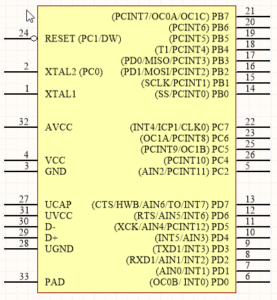
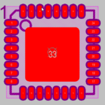
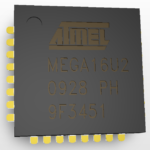
An example of a symbol and footprint for the Atmel Mega chip. Note that if this was posted on-line, it could only be used by those who were using the same tool or a tool able to import the component. Note that importing means translation which is a nice way of saying ‘clean up.’
Millions of components
Although mechanical and electrical design domains each have millions of components available to them, mechanical has the advantage of customization and in-house prototyping. It is easier to have a metal shop, 3D printers, or molding equipment than it is to have a silicon foundry and component packaging facility required to create electronic components. There are few technology companies out there that can take a custom design and put it into a computer chip.
Most companies must select components on the market that are best suited based on functionality, cost, PCB real estate, lead time, etc. It does not mean mechanical has to spend less time figuring out which components are best suited, but they can go in the shop and create a prototype at their discretion. The PCB designers are limited to COTS (Common-Off-The-Shelf) components.
This not only forces the PCB designer to ‘fit a square peg into a round hole’, but the lack of a universal library format also requires the reinventing of the wheel. Currently, if 100 different companies use a particular component, they will each invest precious design time to search for and/or draw the component based on their ECAD tool. This is a massive waste of productivity for the entire PCB industry.
The takeaway from all of this is that the PCB industry needs to address the flow and it boils down to libraries. Right now, every company is or has gone through the pains of pulling together an electronics library and most companies admit that their solution is far from perfect.
The PCB library component creation and its management are a nightmare. Much of this can be remedied by allowing for a universal ECAD format which enables OEMs and suppliers the ability to provide these components to the user. And it is only going to get worse. Whether we like it or not, the age of mechatronics is upon us. If electronic libraries are a hassle now, wait until the mechanical and electronic libraries need to be merged!
Authored by Paul Taubman