Several years ago, Robert Feranec, a well-known video blogger in the printed circuit board industry, was kind enough to post about our PCB Foundations textbook. Our book guides those trying to understand the design process for creating printed circuit boards better. As shocking as it sounds, this medium, which the entire electronics industry relies upon, is not generally taught in colleges and universities! (This absurdity requires a posting all its own.)
Due to Robert’s posting, we were flooded with requests from engineers and designers worldwide hoping to get a copy of the book. Though we were incredibly flattered, and certainly would have liked to oblige, the shipping costs (nearing $200 along with printing) for the 400+ page hardcover book rendered the idea rather impractical.
How else could we impart the book to these customers?
We looked into other distributing methods, namely a PDF, but these options would be easily susceptible to hacking and mass distribution. No matter how we may try to secure the document, “if there’s a will, there’s a way,” especially if there are very limited resources out there. Policing and monitoring hacked copies is rather impractical, if not impossible.
As a result, we decided to turn the physical book into an audiobook video series on YouTube. We used an AI voice narrator that was methodical and clear in English, considering many who requested the book spoke/read English as a second language. We also added closed captions to assist those who struggle with oral English. The pictures in the book were displayed in the videos as the narration progressed. In addition to the images in the book, additional pictures were added to the videos to correspond to the verbiage.
It was a unique undertaking, and by doing so, we accomplished the overall goal of making this resource globally available without compromising our copyright.
If you want to see the videos, click on this link:
When designing Printed Circuit Boards (PCBs), the time to market is crucial – a fact well known to anyone managing these projects. However, what is less obvious is the foundation in which the entire design process rests upon – component libraries. It may sound mundane, but the reality is that poor library management is a leading cause of blown budgets and missed deadlines. Let’s explore why. This insight comes from over 30 years of experience working with dozens of company libraries.
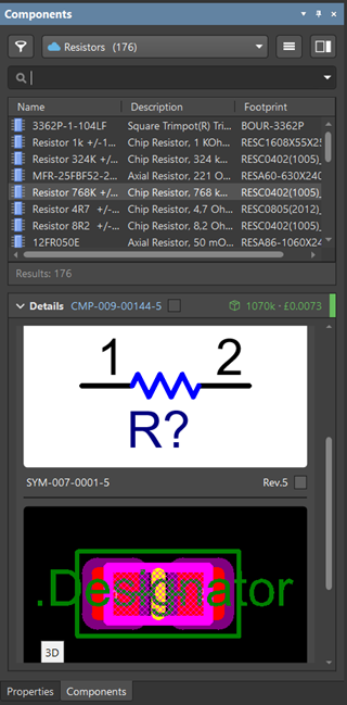
An example of resistors listed in a component library
Understanding How a Component is Used in a Design
Let’s start with a single component. Whether it is a 2-pin resistor or a 2,000-pin processor, in the PCB design process the circuit is drawn twice – once in a conceptual fashion known as a schematic, and the other in a physical fashion known as a layout. When a component is to be used in a design, the component must be defined by two graphical representations (symbol and footprint) in addition to textual information to identify the component in a bill of materials.
An example of a symbol and footprint for a transistor component
Understanding Your Designers
It may surprise you to learn that your degreed circuit designer was never formally trained in the art of PCB design. Undergraduate engineering programs typically focus on learning to design an abstract representation of the circuit, known as schematic capture. Any actual circuit they physically assembled or touched in the classroom labs was limited to protoboards or off-the-shelf completed circuit boards like Arduino, Beaglebone, or Raspberry Pi, to name a few.
Most engineers hired out of college simply forced their way through the tools necessary for the physical layout of the board. They rely on the grit that got them through their academic curriculum to complete the design layout. A new designer must overcome two major obstacles. The first is the learning curve of the tool; these are complex tools that require familiarity with PCB-design terminology to operate in the tool (i.e., polygons, vias, layer stacking, rat’s nests, etc.). The second is designing a board for manufacturing (known as DFM– Design For Manufacturing).
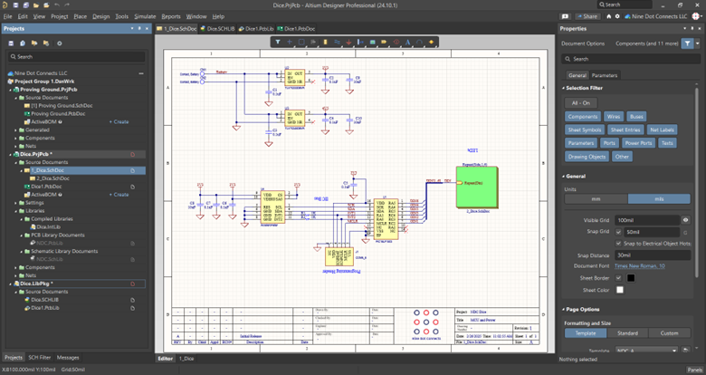
An example of a schematic workspace in Altium Designer, one of the commonly used PCB Design software
Additionally, designers aren’t taught how to maintain a component library, let alone draw a component with its graphical and textural information consistently. Compounding the issue, library management is not trivial and – to be honest – very tedious. Not to mention the other time pressures to create and draw the design itself.
From the Designer’s Perspective.
Let’s now put ourselves in the shoes of an average designer to see how this plays out. We are going to establish a number of assumptions so that we can isolate the underlying issue:
We are familiar with the tools being used for circuit design.
We are competent and capable of designing circuits.
We are capable of getting a design into manufacturing. We have interfaced with fabricators and assemblers and know how to engage them and their expectations.
We have a specification to follow.
The first step in circuit design is to search for the component(s) that will play a key role in this circuit. Our preference is to use components that have we have already used in prior projects.
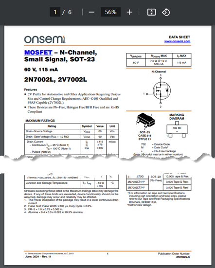
In a well-maintained component library, we should be able to quickly find and place such components onto our schematic design. However, more often than not, we will also need additional components that we have not used in prior designs. We will need to spend time researching components and pouring through their datasheets – some of which rival the size of textbooks. With supply chain issues, there is also an additional task of determining availability.
In addition to researching the component we wish to use, we have the task of defining this component in our software so that we can add it to both our library and our design.
What do we have to define? There are four aspects:
Firstly, we need to textually define the component. This is for two reasons:
Searchability in the component library
Ability to add the information to a Bill of Materials
Textual information includes the manufacturer’s name, manufacturer’s part number, a description, and any key electrical characteristics that define the component. Additional information may be required depending on our company’s workflow.
Secondly, we need to have a graphic of our component for our schematic drawing, known as a symbol. Unfortunately, there is no such thing as a universal graphical component library. It is true that suppliers, OEMs and third parties might provide these symbols; but since every company has its own unique workflow, there is no assurance of accuracy, and every symbol will need to be thoroughly evaluated.
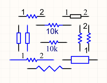
As simple as a resistor may be electrically, its symbolic representation can be expressed in many ways
Thirdly, we need to have a graphic of our component for the physical layout of the circuit, called a footprint. As above, there is no assurance of accuracy and evaluation will be necessary.
Lastly, it is preferable to have a 3D representation of the component so that it may be represented on the board. This allows us to provide a model of the entire circuit for the mechanical engineers to use for fitment into the intended enclosure. This is a critical capability that allows the mechanical and electrical teams to interact without having to redraw the mechanical aspects in two different design tools. Most tools that are used to create printed circuit boards now have the ability to import these 3D models. Note that 3D models may also come from outside sources and will require evaluation.
A 3D model of the previously displayed transistor in both the library (left) and on the layout (right)
Starting Off on a Shaky Foundation
If we pause and look at the duties detailed so far, what we are doing is extremely inconvenient. We are taking top engineering talent and having them delay their design efforts to complete administrative work. For many designers this is a tough mental challenge to deal with, as they’re required to switch between a creative and administrative mindset. By way of analogy, if you are creating a PowerPoint presentation and are absorbed in altering margins, playing with fonts, images, animations, etc. (the administrative work), you aren’t focusing your time and effort on the actual content of the presentation (the creative work).
So then, what should we expect from the average designer? Again, let us put ourselves in their shoes. We have a deadline, and this design will likely have well over 100 components, of which 60% will likely be new. We know that management isn’t interested in component making. They want to see the design process. As a result, we take shortcuts that buy us some immediate short-term gains, but introduce major risk towards the end of the design. Let’s explore some of these common shortcuts:
Blindly copying a component from a prior design.
Asking a colleague if they have the component stashed in their own personal library.
Downloading the component, if available, from the OEM, supplier, or third party.
When all else fails, creating the bare minimum to simply get something into the design.
In this situation, the chances of this component ending up in a company library are slim to none. Even if it is entered into a library, it will not be consistent with other components.
Let’s say that we have completed the schematics with the components we have collected from various sources or created in haste, and we continue along to the circuit layout. This is where the actual copper connectivity is drawn between the components. The component also needs to have a footprint, usually obtained or created alongside the symbol.
The footprint is where the component is going to be soldered onto the board. Unlike the schematic, which is conceptional and dimensionless, the footprint has to be properly dimensioned. As you can image, this is not a place where you want to put blind faith into a footprint that was not vetted. But again, time is of the essence, so these risks are all too often taken.
The previously displayed transistor shown soldered onto the board in 3D Mode (left) and 2D Mode (right)
Where Things Start to go Wrong
The design work thus far has been theoretical. Yes, certain checks and rules can help prevent the absurd, but what we have created up to this point is not physical. This is why the design is moving along as scheduled. Layout delays are typically due to various routing issues between components.
Assuming that we were successful in the placement of components and the routing of copper between them, we now move to fabrication (creation of the board) and assembly (placement of components onto the board). The fabricated boards come from the layout files in the design. The turn-around time for bare boards is usually two weeks, depending on complexity.
In the meantime, we need to pull together our bill of materials. This is where the problems begin. Neglecting review of this list prior to and during layout of the board, any major issues that arise may require us to scrap the fabricated bare boards. For instance, lead time issues might prevent us from obtaining components within our window of need. Avoiding this requires that all (100%) of the components are immediately purchasable, or that approved substitutions can be found. With small components this a common practice, however, when it comes to connectors or components with much functionality, like processors, this would require a major step back.
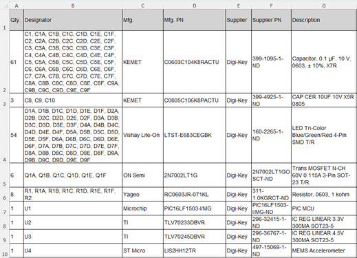
An example list of a Bill of Materials
Even if we do not have issues pulling together our bill of materials and making component purchases, we still have to get through the assembly process. Not only have we invested in board fabrication, but we also purchased components and assembly time. If we did not properly verify the component footprints, they may have incorrect dimensions. As a result, we would have to cease assembly work, review the design and make the necessary changes. Like the bill of materials, the footprints must be 100% correct.
The term “respin” refers to the need to refabricate the board and reassemble it, if the process got that far. The component symbol and/or footprint would need to be corrected and, depending on the component, there may be substantial changes to the layout. The average time it takes to have meetings to discuss the plan of action, to make the changes, and to get it back into manufacturing is at least two weeks.
Keep in mind that as salaried designers, we may feel the workplace stress, but we don’t have the same financial stake in the game as the company does – we’ll still receive our paycheck at the end of the day. Respins ultimately delay the product’s release, potentially causing the company to miss critical market opportunities. Even if the product is eventually successful, there’s a possibility that the profit margin was compromised. Respin costs, the NRE (Non-Reoccurring Engineering) costs, and any additional assembly costs due to work-around complexities caused by design miscalculations all contribute to the loss of the bottom line.
So… Now What?
Now that we have walked through the process and have seen the implications of a poor library, how does a good library prevent this nightmarish scenario?
Let’s consider a library that is well maintained. Firstly, the operative word is CONSISTENCY! A good library does not come about on its own. A company style guide should be adopted and implemented by an individual who owns the library and acts as the component gatekeeper. In an optimal situation, this undertaking should NOT be in the hands of the designers, but rather a technician or another capable, dedicated individual. “Libraries by democracy,” in which all designers have unlimited access to a company library, never work.
Secondly, and just as importantly, a consistent library will provide a clean bill of materials that will literally create itself during the circuit design process. This is possible when each component contains textual information that is consistent throughout the entire library. As a result, the mere placement of these components onto the schematic allows the software to build a bill of materials automatically. In fact, in some companies where the library is well maintained, the design cannot move into the layout stage unless the bill of materials is complete and submitted as part of the design review.
Warning Signs
Take a moment to consider if any of these apply to you and your company:
You do not know if you have a library, or what the condition of that library is.
You ask your designers where they are getting their component and they reply, “wherever I can find them.”
You manually pull together a bill of materials in an Excel spreadsheet.
You manually pull together a bill of materials in an Excel spreadsheet after sending the layout to fabrication.
Your purchasing department has a better understanding of the components used in prior designs than the designers.
The purchasing database has more reliable data about the components than the component library.
If you experience any one of the above issues on a regular basis, it is a red flag that needs to be addressed.
Light at the End of the Tunnel
So, now you find yourself in one or more of these predicaments, or are realizing quickly that these situations are inevitable. If your libraries are in shambles, do not expect your designers to fix them in their free time. Their time is already stretched thin, and even if they did have the time, they do not know how to properly set it up and maintain it. There are simply too many aspects to consider.
At Nine Dot Connects, we have helped dozens of companies get their libraries under control. If you’re tired of missed schedules, blown budgets, and burned-out designers, let us help. We can guide you toward solutions that will streamline your design process and set your team up for long-term success.
Several years ago, Altium decided to stop selling its Concord Pro on-premises database product, and the time has now come when they are no longer renewing licenses for current Concord Pro users. To add insult to injury, once the existing licenses have expired, Concord Pro will stop working altogether, and you will no longer be able to access anything in your database.
Altium provides only one path forward. If you are not willing to put your data on their cloud server and wish to keep it local, you must upgrade to their enterprise database product line. As the name suggests, an enterprise solution’s cost is more significant than Concord Pro’s.
Nine Dot Connects has long supported Concord Pro and its user base. We recognize that the enterprise solution’s high cost will not work for many Concord Pro users. We feel it is an extreme disservice to their Altium customers to force them to choose between an excessive cost increase and total data loss.
Using knowledge derived from years of experience, we can provide several options to help you get out of this bind. In fact, you might even come out ahead of the game if you take advantage of our data cleaning and organizing services simultaneously!
Time is always of the essence, so please get in touch with us as soon as possible so we can help you solve this problem and maintain access to your data.
We at Nine Dot Connects are excited to release our book, PCB Foundations. For grins, we decided to reach out to Steve O’Blenis, the owner of Warbucks Designs, to see what fun he could have with an image or two to promote the book. Steve is a big pop culture/movie fan with a knack for combining different pop culture concepts. Steve provided us with these two images:
Oddly, though Steve did not have a copy of the book when he created the image, page 88 of the 1st edition is the very last page before introducing the design process.
How true, but maybe a bit too edgy…
If you would like to see more of Steve’s work, check out warbucksdesign.com
And, of course, if you would like to purchase PCB Foundations, click HERE:
The present chip shortage has made plenty of headlines in the mainstream press. Where this is most acutely felt is in the printed circuit board design space. Components (a.k.a chips) are electronic functional elements that make up a circuit. They come together on a medium known as the Printed Circuit Board (PCB). These are the green boards you find in your electronic equipment.
In the field of printed circuit board design, there has been a constant clamor to get designers off the imperial unit system known as the mil. The mil is 1/1000th of an inch. It has been used throughout the history of PCB design. Classic component packages like the DIP were designed using the mil for pin spacing.
In the world of EDA tools, there is a factor that may inhibit you or your colleagues from a desire to change to or consider other EDA tools. It is not apparent, yet it is well studied. Your hesitation may be an aspect of procedural memory commonly referred to as muscle memory.
It is the time of the year when companies hire interns for the summer. Let’s face it. Interns are hired to help with the stuff that most designers and engineers do not have the time to address. In our experience, that means libraries. Libraries are the bane of every engineering organization. They are important, but they are time-consuming and tedious. What better activity to give to a greenhorn? Right?
One of the greatest banes of PCB design is the maintenance of component libraries. There are over 1 billion electrical components on the market according to SiliconExpert. Although there are numerous ways of obtaining components, each company must organize their components to fit their needs and workflow.
If you are like most engineers, you may be frustrated with the day-to-day grind of the office place. No one seems to listen to ideas and concerns. No one seems to have the energy or drive to take things to the next level of excellence. Promotions and opportunities never seem to come your way. The extra work and effort are hardly appreciated, if at all. Management seems to be making a lot of money without doing much or even bothering to understand what’s being done.