PCB Photo Gallery
Two of the most significant issues you may encounter when learning about PCB design and manufacturing is the amount of jargon used, along with the incredible number of steps involved from conception to production. We at Nine Dot Connects believe that pictures are critically helpful elements in learning about a field traditionally passed on through tribal knowledge and brute force experience. Even the trade articles and books written about PCB design are difficult to follow without one's ability to visualize what is being explained.
When we wrote our training manual PCB Foundations, we felt it was imperative to provide as many pictures as possible to bring meaning to the text. We also realized that for as many pictures we had in this book, we had many more to share. Thus, we created the PCB photo gallery as a learning tool.
Our objectives for this photo gallery is to show or provide:
- A visual representation of the commonly used jargon and acronyms
- Various physical features of a PCB
- Different manufacturing techniques applied to a PCB
- Interesting design work found on various PCBs.
- The various methods PCBs have been designed through the past 40+ years
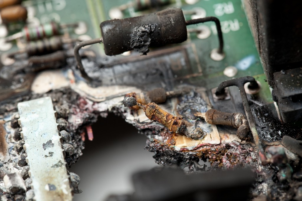
- Issues and concerns that were discovered
None of the images we have taken are from our customer's designs. We took photos of boards we have physically collected from various electronic products over time.
The pictures are royalty-free. If you would like to use any of the images found in our gallery, please provide the following statement adjacent to the picture. "Image is courtesy of ninedotconnectssandbox.com. The use of this picture is not an endorsement by Nine Dot Connects, LLC."
I was particularly pleased to have this gallery available for our ECAD librarian's perusal. She's new to the PCB design and manufacturing business, and I'm doing my best to provide the context she needs to do her job effectively. It really helped.
Our PCB Designer, EE, the other senior tech on my staff, and I all appreciated seeing some of the "problem children" in the gallery as caveats to our work. And, was interesting to see some of the more advanced designs as "waypoints" for our work going forward.
William Letendre, EE Manager, Airmar Technology Corporation
