- Nine Dot Connects
- Webinar of the Month
- Recently Posted Videos
- Altium Designer (70)
- Cabling & Wire Harness (5)
- Design for Manufacturing (10)
- Fabrication & Assembly (9)
- ECAD & MCAD (7)
- High Speed Design (20)
- Library Management (18)
- Vault & Data Management (16)
- PCB Broadview (4)
- PCB Elements (16)
- Power Supplies (5)
- Simulation (12)
Advanced PCB Footprint Creation Techniques
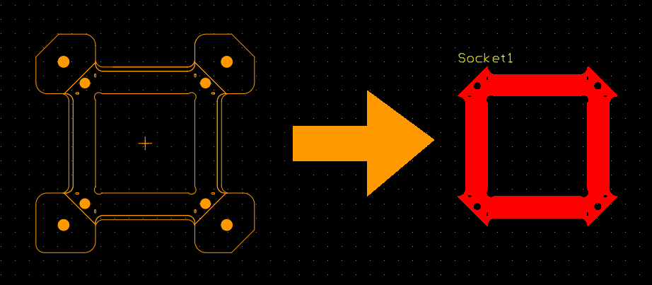
Most footprints you need to make in Altium Designer can be created using the PCB wizard or taking advantage of footprint symmetry. However, some footprints are unusual in shape and need a different design approach. In this webinar, we will explore:
- The capacitive touch library provided in Altium Designer
- Using DXF/DWG files as molds for a footprint
- Using polygon pours to create regions that can be used for footprint pads
- Using a script when an algorithm-based footprint must be created
Learn More

