- Mental Amusement
- The aXe Files
- The Rust of Yesteryear
A Guide to Mechanical Layer Configuration
We will start by stating that there is no official standard when it comes to mechanical layers. Several years ago, there was an effort by Darren Moore, an expert user of Altium Designer, who compiled a list of all the unique mechanical layers that designers have used to represent key elements of their designs. The list contained over 42 different layers!
Would one need all 42 of these layers? This is not the case. The layer set presented in this writing may be more than necessary.
With a few exceptions, the purpose of the mechanical layers is to convey human-readable information. Though the manufacturing of the PCB is highly reliant upon machine formats such as Gerber or ODB++, these formats do not convey all of the needed instructions. Several manufacturing issues have their roots in the lack of information being passed along.
The purpose of this paper is to guide you along a reasonable path so that a robust set of layers can be established for your company, in addition to setting up the layers so that it is easy to assemble one's documentation.
The list presented is simply an example. The order, the colors, and the names are up to the company. However, as with all library components, consistency is crucial. Therefore, whatever is established for your company should be agreed upon by all and followed thereafter.
Mechanical Layer Names
When it comes to names, there is a need for consistency. In the example above, all mechanical layer names start with the format 'M##.' In most EDA tools, the user can rename the mechanical layer; however, that's simply an alias for its real name that the system will use in its. Therefore, starting with the prefix of the original mechanical layer name allows you to quickly translate between the purpose of the mechanical layer and the actual name of the layer.
In the above example, no white spaces were used. The details of the name are separated by an underscore ( _ ). This was done for two purposes. First, it simply makes it easier to discern between the three fields of information within the name. In this example, there are three fields, the first represents the mechanical layer number, the second provides a brief description, and the third, if used, provides whether the top or the bottom is being viewed.
Second, the use of the underscore is a safeguard against a sneak attack of the metacharacters. Those familiar with programming know that nonalphanumeric ASCII characters (i.e., !@#$%^&, etc.), especially white spaces, can be used as record separators, delimitators, or operators. Though using these metacharacters may work fine for your EDA tool, importing your documentation into another format processed by another software program may cause some issues.
Even EDA tools themselves are not entirely immune. We must remember that features and functions that may make use of these names may have been written differently by different individuals. Therefore, the coding for a particular feature or function may not be robust to handle these metacharacters.
Therefore, when it comes to names - net names, component names, stack-up names, class names, mechanical names, etc. - stick to the classic programmers' convention of alphanumeric characters and the underscore ( _ ) to avoid any sneak attack of the metacharacters.
If multiple words describe the layer, they are combined without white space, using a capital letter to start the next word. (In the case of an acronym, one may use the lowercase letter. For example, the layer name 'PCBoutline' is easier to read, with the second word being lowercase.)
As for the description, the key element is to make it readable. Abbreviations are fine as long as one can surmise what the layer represents. In the example above, one could have used 'CompMech' instead of 'ComponentMech.'
The name's suffix calls out the top or bottom layer if applicable. Logically speaking, one should keep the corresponding layers next to each other in order and not flip the order. For example, if the top layer for a particular mechanical layer is called out first, the bottom layer should be called out immediately thereafter. This pattern should be repeated for the other layers.
Mechanical Layer Colors
When it comes to colors for the mechanical layers, they are true to the eye of the beholder. Though a template may come with a specific set of colors, the user can change these. In the end, the documentation files are formatted into text or printed in black and white images. The only exception is the production of 3D images, another color palette altogether.
There are two thoughts to consider when dealing with colors.
- Use colors that will contrast to the background. The best background color is black, given that most other colors will contrast to it.
- It is okay to reuse colors. If you do, be strategic about which mechanical layers may share the same color. For example, if the mechanical layer for notes and the mechanical layer for the stack-up share the same color, the information being displayed should be evident as to which layer it is associated to.
Mechanical Layer Pairs
Most PCB tools can match the layers. This is especially useful for matching layers representing the top and bottom of a particular layer representation. By default, a component is always created in the library from the top layer perspective, and the component is initially placed on the top of the PCB layout. When the component is flipped to the bottom side, the PCB tool should be able to transfer mechanical information to the bottom side.
Layer Details
The following is a list of layers that one may wish to consider. Note that not all of the layers one may desire are listed, nor does one need to use the layers that have been listed.
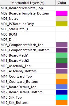
- M01_BoardTemplate_Top. The title block and border. Only information about all layers should be placed on this sheet. When printing or creating PDFs that do not require mirroring, this sheet should be turned on as one of the layers.
- M02_BoardTemplate_Bottom. The title block and border in reverse. This is used when mirroring any of the layers in the printout. Ensure that whatever information was added to the M01_BoardTemplate_Top is also added to the M02 template sheet. Enable this layer and the mirror option when printing or creating a PDF for the bottom of the PCB. This becomes a 'mirror of the mirror,' allowing it to be read.
- M03_Notes. This page should contain all the keynotes for the fabrications and assembly of the design. Other notes may be allocated to other specific pages, as warranted. Like M01 and M02, the note page is for human readability.
- M04_PCBoutlineOnly. This layer should only contain the outline of the PCB (including cutouts) and nothing else. It should not contain the template, notes, or dimensions. The fabricator uses this to obtain specific dimensions of the board. The fabricator and assembly will erase any additional information on this layer.
- M05_StackDetails. This layer contains layer stack-up information.
- M06_BOM. This layer contains the BOM. Though normally not done when the board contains hundreds of components, it makes it convenient for smaller boards to be a quick visual.
- M07_Drill. This layer contains all of the drill information, including via types. Note that through graphics like the drill plot can be placed on this layer, separate NC drill files can assist in drilling.
- M08_ComponentMech_Top. Used to assist with the 3D bodies and STEP component projections on the top layer. The library footprints should conform to this layer for 3D component bodies (which includes STEP). This layer should be matched to layer M09.
- M09_ComponentMech_Bottom. Used to assist with the 3D bodies and STEP component projections on the bottom layer. This layer should be mechanically matched to layer M08. If a component is flipped to the board's bottom side, the body should also be moved from M08 to M09.
- M10_BoardMech1 - This should be used for any 3D bodies and STEP component projections related to the board that is not associated with the footprints.
- M11_BoardMech2 - This should be used for any 3D bodies and STEP component projections related to the board that is not associated with the footprints.
- M12_Assembly_Top - Assembly layer shows the centroids of the component and pin 1 location for the top of the board. The library footprints should conform to this layer. This layer should be matched to layer M13. Additional notes and information can be added to this layer.
- M13_Assembly_Bottom - Assembly layer shows the centroids of the component and pin 1 location for the bottom of the board. This layer should be matched to layer M12. If a component is flipped to the board's bottom side, the assembly information on M12 should also be moved from M12 to M13. Additional notes and information can be added to this layer.
- M14_Courtyards_Top - Courtyards assist in the initial placement of the components. Unlike 3D bodies, they can account for necessary spacing for egresses and other mechanical needs. This layer should be matched to layer M15. The outline of the board should be drawn. Additional notes and information can be added to this layer.
- M15_Courtyards_Bottom - Courtyards assist in the initial placement of the components as described for M14. This layer should be matched to layer M14. If a component is flipped to the board's bottom side, the information on M15 should also be moved from M14 to M15.
- M16_BoardDetails_Top - Any dimensions or details specific to the board's top are entered on this sheet.
- M17_BoardDetails_Bottom - Any dimensions or details specific to the board's bottom are entered on this sheet.
- M18_Silk_Top - Though the top silk is given its own layer in most PCB tools, this layer allows additional information to be added without impacting the silk layer itself.
- M19_Silk_Bottom - Though the bottom silk is given its own layer in most PCB tools, this layer allows additional information to be added without impacting the silk layer itself.
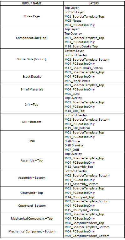
Layer Grouping
As one can imagine, with each of these layers having a specific function, it may be difficult to enable the proper layers to get the whole picture. A good EDA tool will allow the user to group layers so that there is a complete representation of the concept.
Formatting the Mechanical Layers a Fabrication Format
In general, there is no issue with converting the mechanical layers into one of the fabrication formats (Gerber, ODB++, or IPC-2518). Just understand that most of the mechanical information will be discarded when prepping the equipment for fabrication. The key layers used for fabrication are the signal, plane, and dedicated layers, such as silk or paste.
What's the point of using mechanical layers? They provide human-readable instruction. More so, some notes and instructions are often not captured in the design itself or the machine formats. The mechanical layers detail these essential concepts.
