- Nine Dot Connects
- Webinar of the Month
- Recently Posted Videos
- Altium Designer (70)
- Cabling & Wire Harness (5)
- Design for Manufacturing (10)
- Fabrication & Assembly (9)
- ECAD & MCAD (7)
- High Speed Design (20)
- Library Management (18)
- Vault & Data Management (16)
- PCB Broadview (4)
- PCB Elements (16)
- Power Supplies (5)
- Simulation (12)
Practical Aspects of Signal Integrity - Part 3
"There are two kinds of engineers: those who have signal integrity problems and those that will." - Eric Bogatin
In parts 1 and 2 of our webinar on "Practical Aspects of Signal Integrity," Tom Cassidy provided the basic design concepts to consider when laying out a board for high-speed signals to ensure the signal's integrity. If you missed one or both, we encourage you to watch the recording of these webinars. The concepts presented build upon each other.
Watch Part 1
Watch Part 2
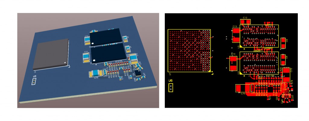
In Part 3 of this webinar series, Tom will present the simulation and analysis of a functional FPGA-based DDR3 memory design. He will also examine some common layout paradigms inherent to DDR3 and explore their signal integrity implications.
- Xilinx Zynq FPGA and Micron DDR3 Memory
- "Power-aware" Simulation and Analysis
- JEDEC Compliance Reports
- Signal Termination
- Differential Pair Routing Concerns
- Alternate Routing Paradigms
Although this webinar will use a board designed in Altium Designer and analyzed in Cadence Sigrity, the concepts apply to any tier-one analysis tool.
Learn More

