Simulation for DDR3/DDR4 Design
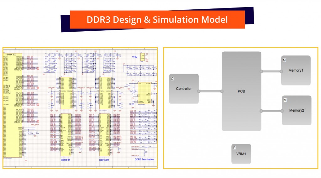
We can assist with any or all of the DDR3/DDR4 design and layout steps, doing as much or as little as you need, everything from simple design reviews to full-on turnkey layouts, even if it is just the DDR3/4 portion of your project. Below are the steps of the process and the services provided in each step. We understand that this may overwhelm those new to DDR3/DDR4. We encourage you to contact us if you need assistance with what is being offered.
Initial Design
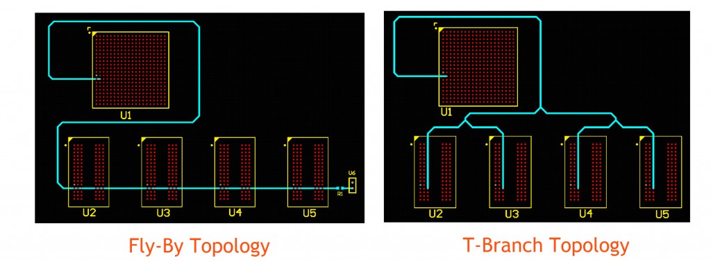
- Memory device selection, termination schemes, routing topology (fly-by vs. T-branch), differential pairs, proper power, and decoupling
Design Review of Existing Designs
- Proper interface to the memory controller, FPGA pin usage, controller pin package delay calculation, bit swapping, reference voltages, impedance control
PCB Layer Stackup
- Number and type of layers, use of microstrip vs. stripline, symmetric vs. asymmetric striplines, PCB material, and dielectric constants
Design Rules
- Proper dimensions for correct impedance control, size, and use of vias, correct rules for different layers, signal group classes, Altium "xSignal" setup
High-Speed Routing
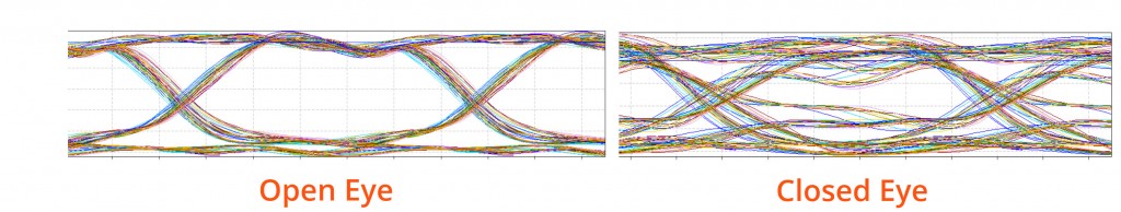
- Correct signal timing using "delay tuning" vs. just trace length tuning, clean routing for best signal integrity, pin swapping, correct use of serpentine traces, the proper return current paths, correct usage of reference planes
Design Verification
- Use both commercial and proprietary tools to verify the final design and layout, analysis, and feedback to the customer