DDR3/4/ & LPDDR4 Design & Layout
DDR (Double Data Rate) memory configurations are constantly evolving. With each iteration of the DDR specification, chip providers find faster ways to move data to and from memory. Their approach is twofold - to increase the speed on the memory component and then find configurations that increase the speed between PCB components.
The function of memory is to provide a stored data location to the component processing the information. Although microprocessors are an excellent example of a component that extensively uses external memory, other devices such as DSPs (Digital Signal Processors) and FPGAs (Field Programmable Gate Array) also use external memory.
Regardless of which component uses the memory, the routes between the processing component and the memory device(s) must be properly designed. The two concerns are propagation times and signal integrity. The signal cannot arrive late in a non-readable condition.
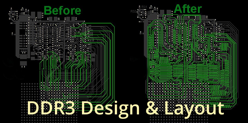
3 Banks of DDR4s, 3 large FGPAs, and 96 Pairs of 15 Gbps Signals Design
Performed by Nine Dot Connects
Nima Badizadegan, EE - Calliphony
Memory configurations have changed through the years to optimize the throughput of the data to and from the memory device(s). DDR (Double Data Rate) takes advantage of both the rising and falling edges in a clock cycle.
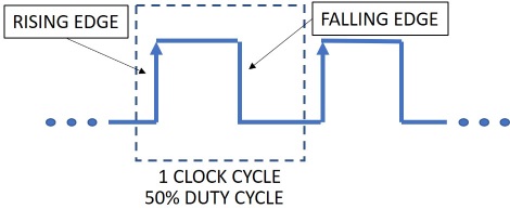
In the past, memories only operated on the rising edge of the clock. Now that both edges are employed, any setup for the next signal, whether inbound or outbound, must be ready when the next edge occurs.
DDR3 is currently the industry standard. However, DDR4 is entering the industry, especially gaming computers. The PCB layout must handle strict timing requirements regardless of the DDR version while maintaining signal integrity. This is not an easy task.
The following is an outline of the strategy Nine Dot Connects uses to design a DDR board:
Initial design (Schematic)
- DDR3 Memory device selection
- Termination schemes
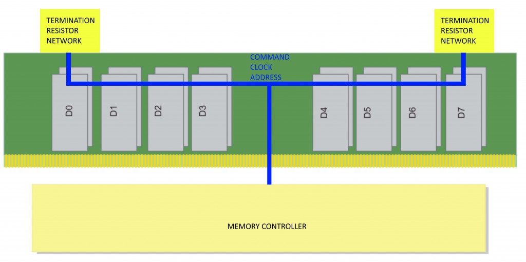
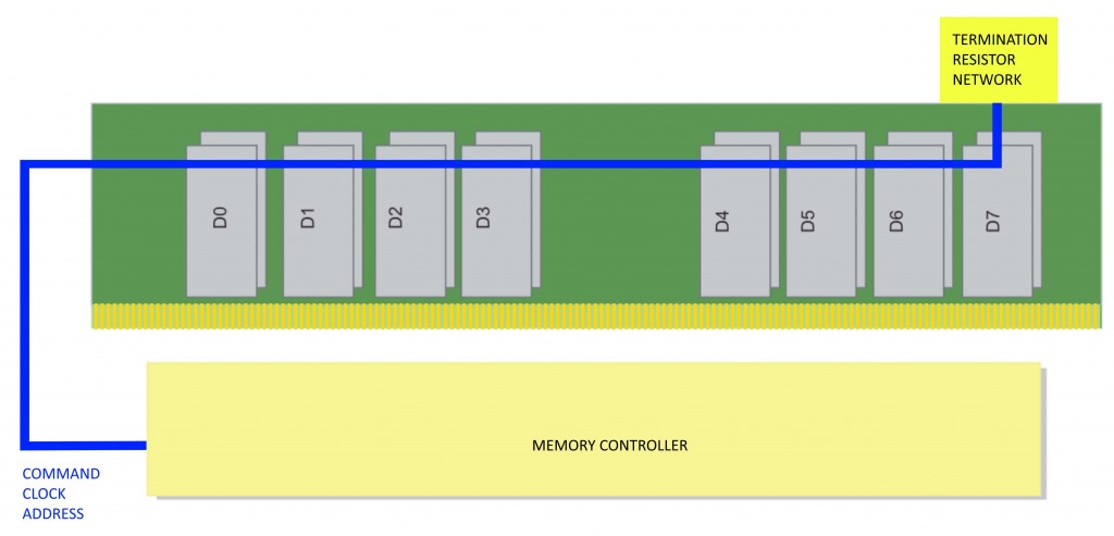
- Routing topology (fly-by vs. T-branch)
- Differential pair declaration
- Power and decoupling considerations
Processor Component consideration
- Memory controller interface concerns
- Pin usage (if FPGA)
- Controller pin package delay calculations
- Bit swapping of data for optimal routing paths
- Reference voltages
- Impedance control
Layer stackup
- Number and type of layers
- Use of microstrip vs. stripline
- Symmetric vs. asymmetric striplines
- PCB material and dielectric constants
Design Rules
- Proper dimensions for correct impedance control
- Size, type, and use of vias
- Custom rules for different layers
- Signal group classes (and use of Altium "xSignal" setup, if applicable)
High-speed routing
- Calculate signal timing using "delay tuning" vs. just trace length tuning
- Routing for best signal integrity
- Pin swapping (if FPGA)
- Proper use of serpentine traces
- Return current paths
- Correct usage of reference planes
How can Nine Dot Connects help you with your DDR3, DDR4, or LPDDR4 design? We can assist with any DDR design and layout steps, doing as much or as little as you require. Everything from simple design reviews to full-on turnkey layouts, even if it is just the DDR portion of your project.
Contact Us
The following is an overview of what one needs to do when designing DDR3 onto a PCB:
Schematics
DDR starts with the initial design before the layout. Memory components must be selected, as each memory manufacturer has its own requirements and recommendations. The routing topology (fly-by vs. T-branch) must be considered when drawing out the schematics circuit. Each topology type has its advantages and disadvantages.
These details will determine the component placement on the PCB. The schematic will generate the netlist for the PCB layout designer to follow during the trace routing between these components.
FPGAs
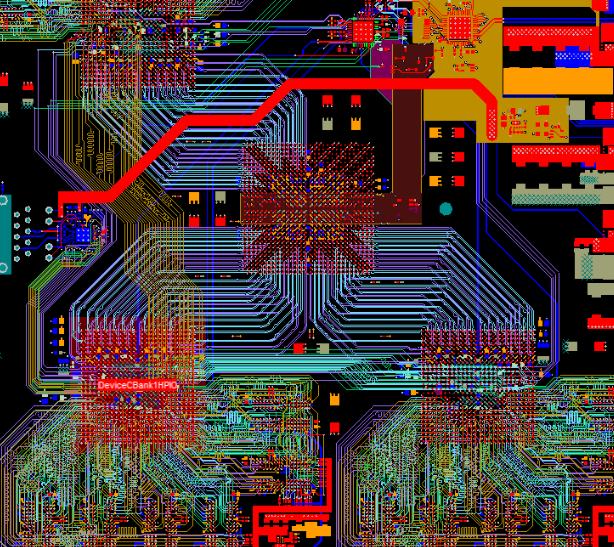
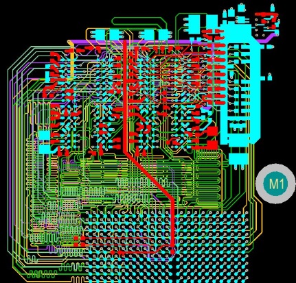
In many cases, DDR memory will be interfaced with an FPGA. Because they are configurable, the circuit board designer must balance the internal logic utilization aspect of the FPGA with the signals assigned to each of its pins. There can be hundreds of pins on one FPGA.
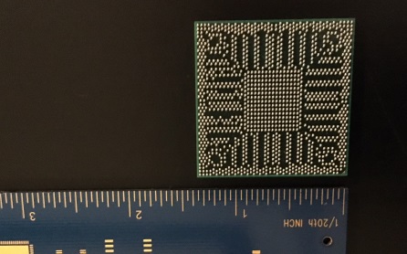
Example of a 1299 Pin BGA
What may look good on the schematics and work internally in the FPGA could be a routing nightmare in the PCB layout. Because FPGAs are configurable, pin swapping is permitted to alleviate the routes from crisscrossing or being too far distant from each other. However, this can impact FPGA's internal timing.
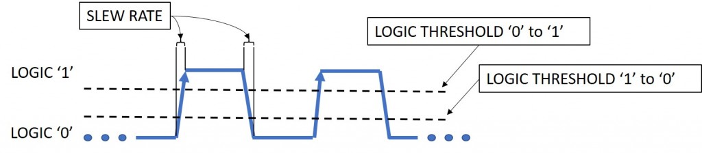
This is an iterative process of swapping pins, performing impact checks on the FPGA, and modifying the schematic. Other aspects of the FPGA, such as slew rates (the speed in which the signal goes from logic '1' to logic '0' and vice versa), voltage levels (the voltage level required for a logic '1' signal), and propagation delays (a.k.a. timing delays) that can be configured for each pin, must also be given consideration.
Layout
The layout of the board is a significant factor in the design. The number of layers (a.k.a. the stack up) will determine each layer's impedances. Impedances must be matched while routing the DDR memory signals to avoid signal integrity issues. The number of signal layers is not the only consideration. Planes of copper must also be considered to assist the signal propagation through the trace and minimize electromagnetic field interference between signal paths. The non-conductive material (a.k.a. dielectric) that separates the copper layers is critical in the impedance calculation.
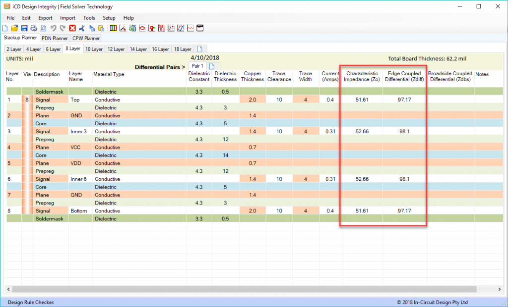
The designer works closely with the board fabricator to perform impedance measurements. Based on the criteria described above, the fabricator can provide the preliminary impedance numbers to assist the designer during the routing process. Additionally, the iCD planner allows the designer to calculate further impedances based on the layers used, the desired trace widths, and the spacing between traces.
Design Rules
The layout of the board is constrained using rules. These rules prevent the layout designer from placing routes that would cause signal integrity issues. They also dictate constraints such as trace width and spacing, component clearances, and differential pair spacings derived from the physical board's stack-up, as described above.
Placement of Components
Component placement is critical to minimize congestion between DDR memories and the processing component. Topography selection during schematic entry will dictate a good portion of the placement.
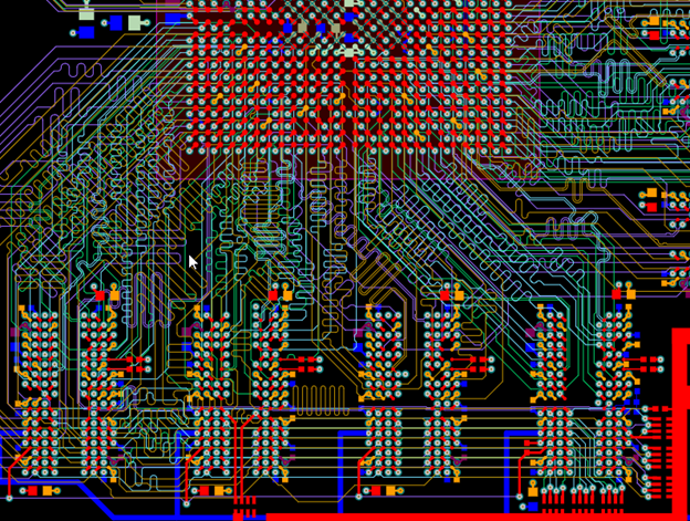
Routing
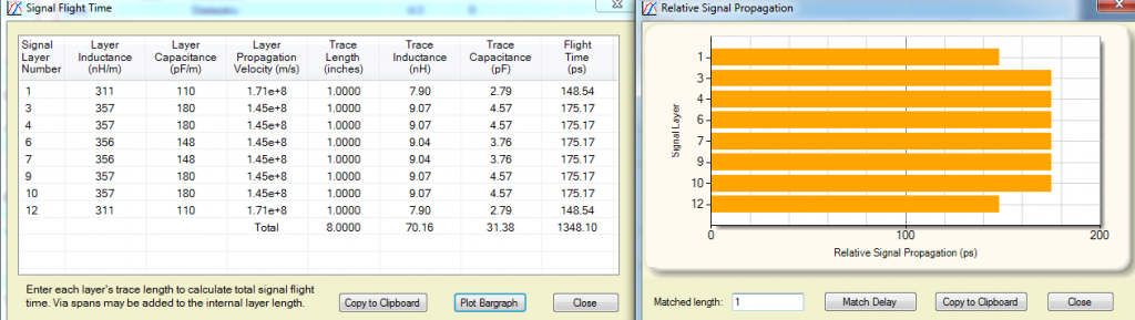
The objective is to ensure the routes match timing requirements. This also requires understanding how different layers impact the signal propagation speed. The propagation time for one layer is not the same for another. The designer must translate the propagation time into a wire length.
Since high-speed signals are involved, one cannot neglect the field energy produced when a signal goes from logic '1' to '0' or vice versa. It must be 'channeled' appropriately; otherwise, it will radiate as noise, bleed onto other routes, and harm the signal itself. Voltage planes must be correctly referenced, and return paths must be absent of copper voids.
Serpentines are employed to assist with match length tuning and propagation delay
In Summary
This process should not be rushed. Each decision made on the board must be made with careful consideration. The components need to be placed in an optimal configuration. Each route must be fine-tuned to meet the timing requirements. Proper methods must be employed in high-speed design to mitigate noise and maintain signal integrity. In this brief strategy discussion, we purposely neglected to mention other essential items, such as via type and size, drill pairs, and decoupling requirements, to name a few.
To showcase the necessary steps involved in properly designing with DDR3 memories, we conducted two-part webinar series. You can find details on this series here.
DDR3 Webinar Series
How can Nine Dot Connects help you with your DDR3, DDR4, or LPDDR4 design? We can assist with any DDR design and layout steps, doing as much or as little as you require. Everything from simple design reviews to full-on turnkey layouts, even if it is just the DDR portion of your project.
