- Overview
- Library Service Options
- Library Clean Up
- Library Sustainment
- Librarian On-Demand
- Quote Request
- Why Conformity Matters
- Ugly Components
- Symbol Style Guide
- 3D Model Included
- Library Intro/Philosophies ⇩
- SVN (or GIT) Library
- DFM Library Example
- Library Resource Videos (18)
- Avoiding Gotchas
- Altium Vault Services
- Altium 365 and its Evolution
- Configuration Setup ⇩
- Life After Concord Pro
- Vault Management Videos (16)
- Overview
- Point of Entry
- L9 Videos (4)
- L9 vs. Vault
- Evaluation
Symbol Style Guide
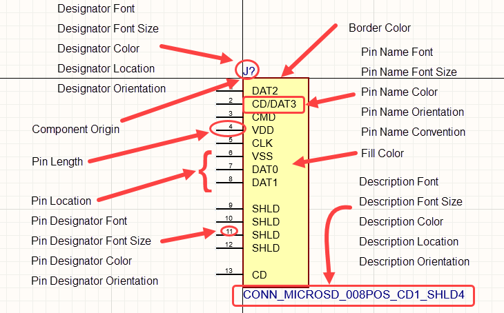
When working with symbols in PCB designs, it is important to have guidelines for their creation. Without guidelines, many problems can arise, from (but not limited to):
- Parts being on different grids and not connecting properly in the schematic
- Difficulty in reading the flow of the schematics
- Redundant components in the library leading to confusion as to which to use
If guidelines are not established, it is practically guaranteed that companies will run into problems down the line that require a lot of effort and time to get their libraries cleaned up. Therefore, guidelines should be established from the start.
The purpose of this commentary is to recommend some guidelines for creating symbols. While it is not imperative to follow all that is recommended in this guide, it is important that some sort of guideline be established and followed to have a consistent and cohesive library.
Keep in mind that all the properties listed in this commentary are just examples and suggestions, but if they are followed then the result will be clean and efficient component libraries.
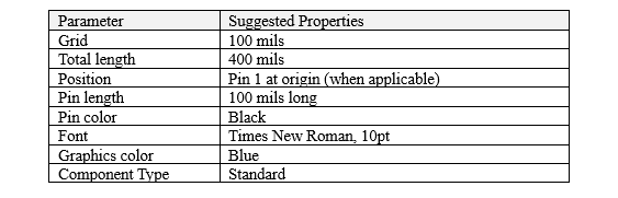
GENERAL GUIDELINES
GRIDS
This style guide breaks the symbols into two distinct categories: discrete components and ICs. The symbols for the discrete components follow the IEEE and ANSI guidelines. While most ICs will have unique symbols, some simple rules can be established that will make them more uniform which results in them being easier to create in the library and more readable on the schematic.
Using a consistent grid size when creating symbols and schematics is essential. It ensures that components will line up properly for wiring connections to be made. If two different symbols are made with different grid sizes, the wires may not connect with the pins. Note that all the symbols defined in this guide use Altium Designer's default grid size of 100 mils.
Though the use of the imperial system may bother some who are strongly against it, it is important to keep in mind these aspects:
- By their nature, schematics are conceptual and dimensionless. For example, a 1.5in X 1.5in BGA with 1000+ pins can take up five or more schematic sheets. In short, we simply cannot use dimensions in the schematics for size or distance.
- Though it may be an excellent way to weed out outside components that have not been vetted in your library, all third-party suppliers provide Altium components using the 100mil grid.
PIN ELECTRICAL TYPE
Altium Designer allows the user to declare the electrical type of pin such as passive, power, in, out, bi, etc. This is to assist with the ERC (Electrical Rule Checker) that runs when the netlist is being generated or updated in the schematic editor. Though it is nice to have, they take time to establish when creating a symbol and the return of time investment is questionable. A good designer would generally avoid the mistakes that would be flagged by having pins set to their proper electrical type. That said, if you are designing for Class-C (mission critical), then this is one more check to verify that a fundamental mistake is not being made. Keep in mind that the ERC is only checking for netlist issues and knows nothing about the components that are being connected to each other in the schematic.
COLOR SCHEME
The coloring should be consistent throughout the library. In this guide, the following are used:
- Black is used for the pin color.
- The default "Altium" blue (RGB 0-0-255) is used for the human-readable graphics.
- The default yellow (RGB 255-255-176) is used for rectangles (used in ICs and connectors).
- The default dark red (RGB 128-0-0) is used for the rectangle borders.
- The default dark blue (RGB 0-0-128) is used for text, parameters, and designators.
FONTS
Times New Roman, 10pt. is used for all the symbols as a simple and clear font choice. Alternatively, many companies use Arial.
PIN TEXT VISIBILITY
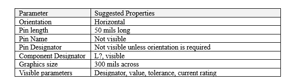
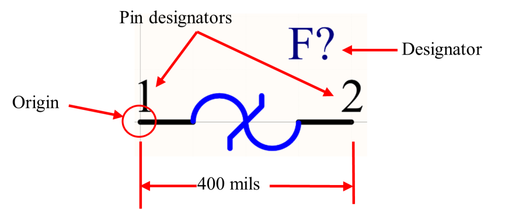
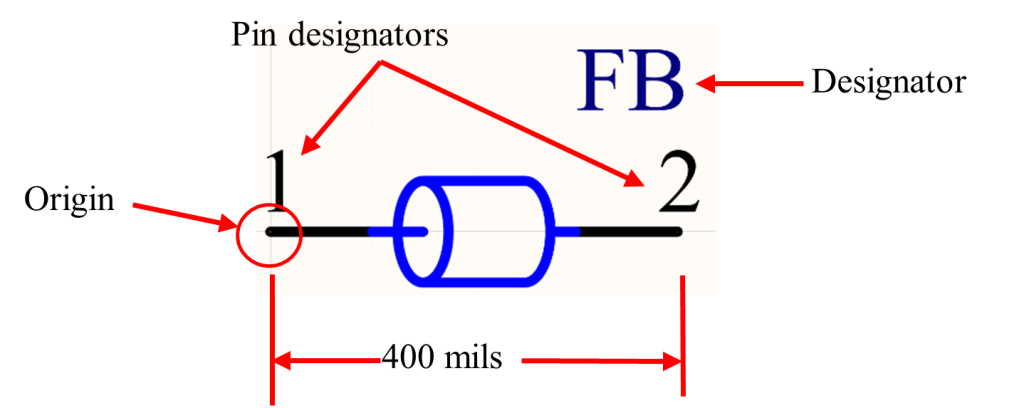
There are two textual properties of a pin, the name and the designator. Depending on what type of component is being created, either one of these may be shown or hidden. In the images used for the following examples in this guide, pin numbers are displayed for placement preference purposes. Refer to the tables below each category to determine pin number and designator visibility.
In general, the following apply:
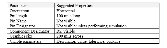
- For discretes, both the name and the designator of the pin are hidden, unless orientation is critical. For example, a diode has orientation that must be followed.
- For ICs, both the name and designator are visible for each pin.
- For connectors, only the pin number is visible, unless the connector is for a specific standard or protocol such as PCI, SATA, USB, etc.
GENERAL SUMMARY
For this guide the following applies unless otherwise noted:
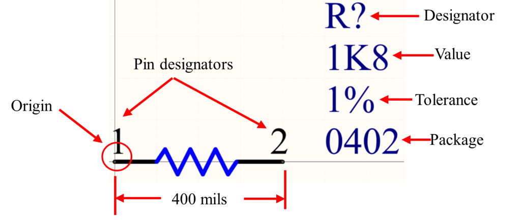
DISCRETE COMPONENTS
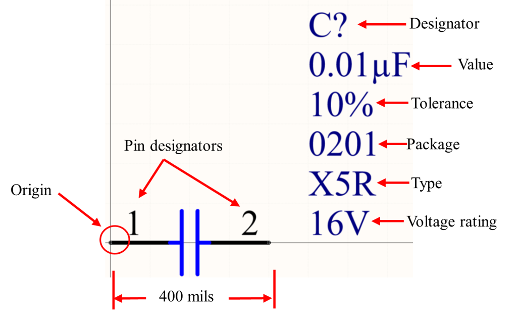
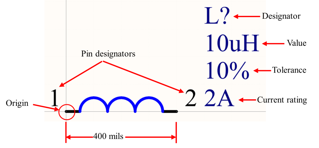
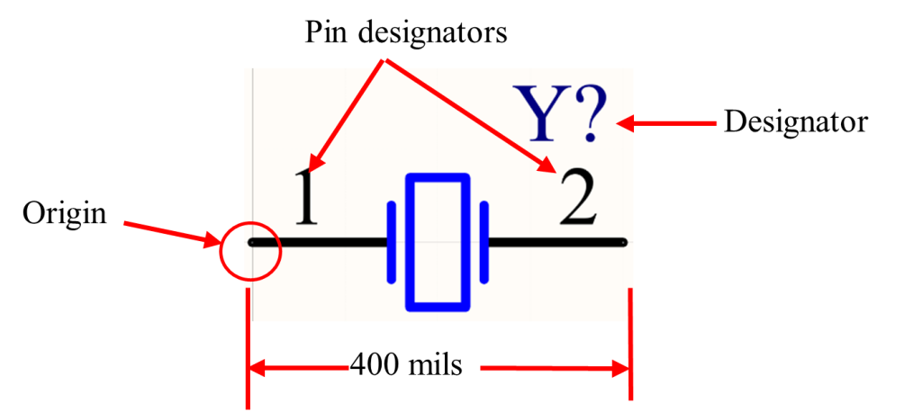
All the two-pin discrete components (such as resistors, capacitors, inductors, etc.) should be made with the same width. This allows the components to align properly when placed on the schematic. Experience has shown that making all the two-pin discrete components 400 mils wide is optimal for fitting the graphics of each symbol between the two pins.
1. RESISTOR
2. CAPACITOR-NON-POLARIZED
3. CAPACITOR-POLARIZED
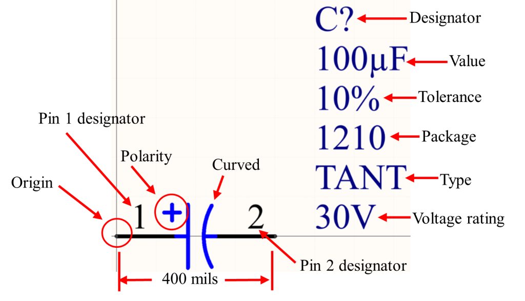
The symbol for the polarized capacitor is generally the same as for the non-polarized, except that the polarity marking (+) is shown on pin 1 in blue graphics, and the graphical line on pin 2 is curved toward pin 1.
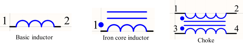
4. INDUCTOR
5. DIODE
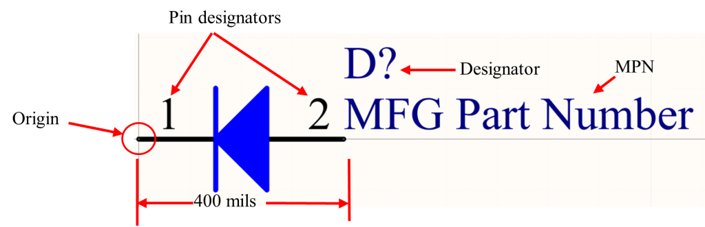
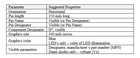
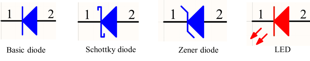
Note: An alternative to using pin numbers is to use the type of pin such as 'A' for Anode and 'C' or 'K' for Cathode. By using these letters rather than numbers, the orientation of the diode is clearer. If using alpha conventions for the pin designators, remember that the footprint pads need to match the pin designators.
6. CRYSTAL
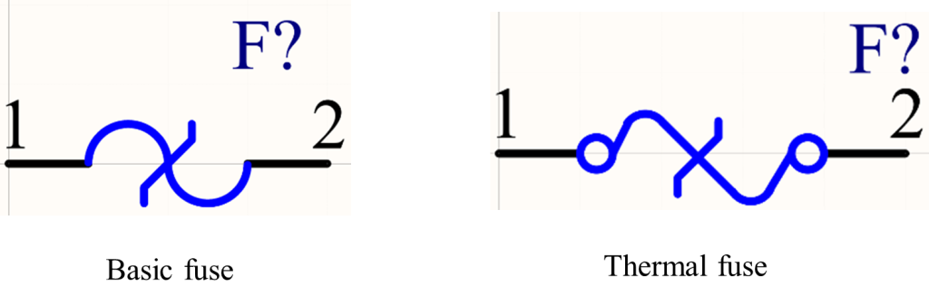
7. FUSE
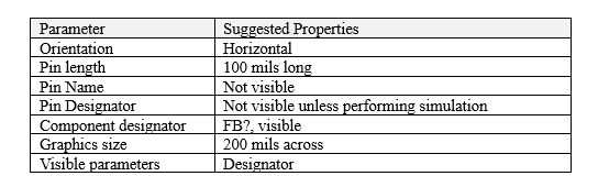
8. FERRITE BEAD
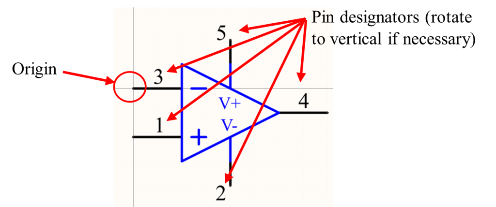
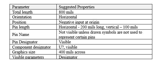
9. OP AMP
10. TRANSISTOR
Note: Given that pins 1 and 3 can be assigned differently for the collector and emitter, an alternative pin designator form would be to use 'E' for the emitter, 'C' for collector, and 'B' for the Base. Similarly, you may use 'S' for Source, 'G' for Gate, and 'D' for Drain on FET components. If using alpha conventions for the pin designators, remember that the footprint pads need to match the pin designators.
11. SWITCH
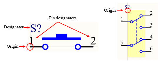
If the switch has more than two pins, then the top left corner of the rectangle is placed at the origin with the symbol running vertically. The width of the symbol will vary depending upon the type of switch. It is custom to draw out the switch configuration when creating a two or more pin symbol.
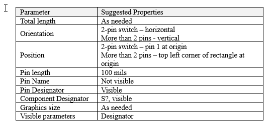
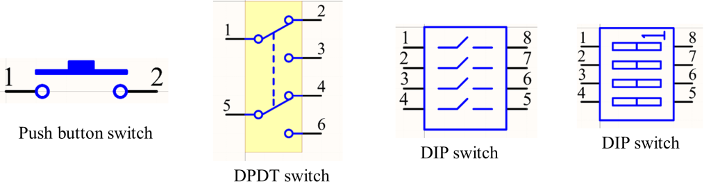
For single pole, single throw switches, the symbol should represent the default setting of the switch. For example, the push button switch shown above would be interpreted as being off by default. If the switch was on by default, the top line would be drawn touching the two contacts.
Another way to identify the default setting is to add the letters NO (Normally Open) or NC (Normally Closed.)
CONNECTORS
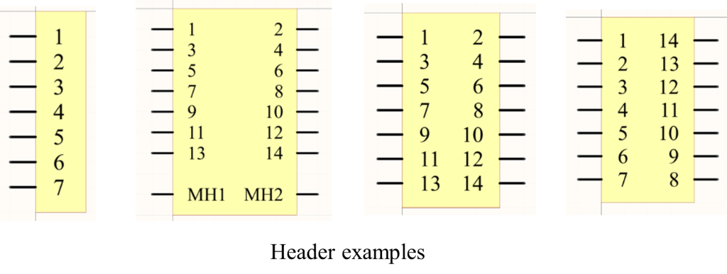
1. CONNECTOR-HEADER
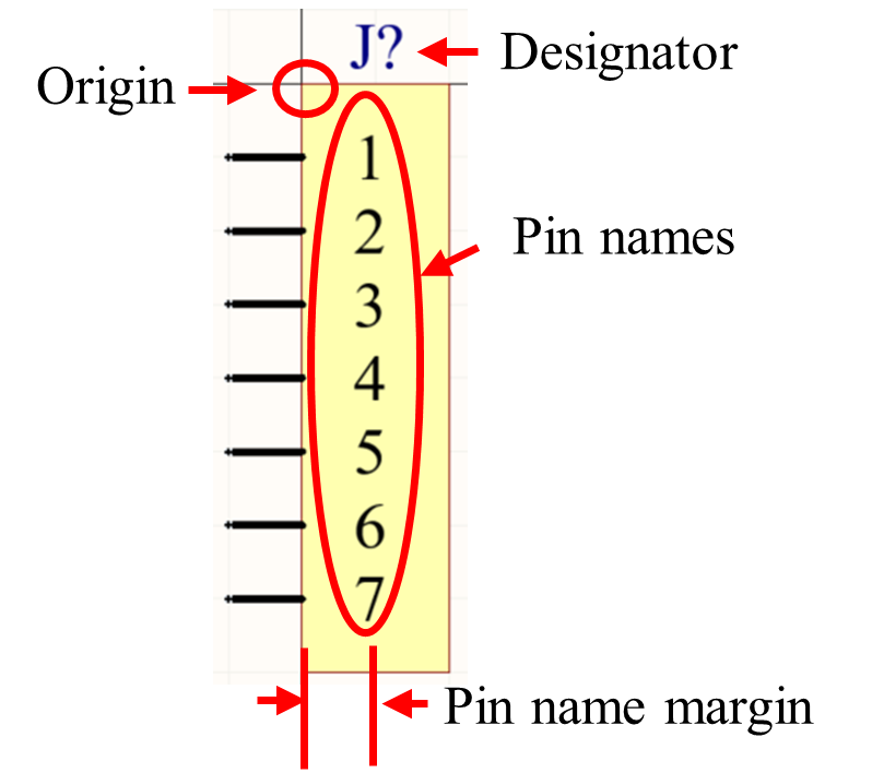
If a single row header, all the pins are aligned on the left-hand side of the rectangle. If a double-row header, then the pins are on both sides of the rectangle, numbered as they are on the connector. The pin designators (numbers) are not visible, but the pin names are since both designator and name are the same. If the symbol is longer than half the paper size, it is broken into multiple symbols, such that none of them are more than half the paper size commonly used by your company. (Paper sizes: A-size - 7500 mils; B-size - 11000 mils; C-size - 17000 mils; A3-size - approximately 11700 mils)
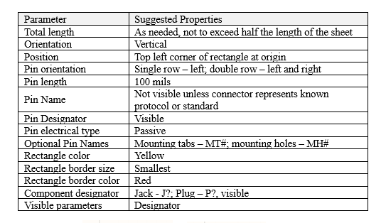
In regard to the features of the connector that may go through the PCB to provide support, they may be represented as pins on the schematic if they can be soldered. The soldering of these pins permanently attaches the connector to the PCB in addition to providing a path to ground, if warranted. Plastic pins should not be represented as pins. The holes needed for plastic features going through the board will need to be accounted for in the footprint itself.
2. CONNECTOR-OTHER
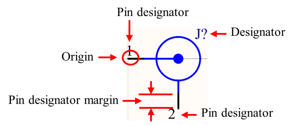
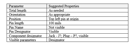
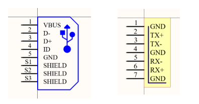
Connectors that are not headers (such as D-sub, coax, USB, etc.) should be drawn to best represent that style of the connector. These symbols are oriented with the top left pin at the origin. The pin designators are visible, but the pin names aren't since both designator and name are the same.
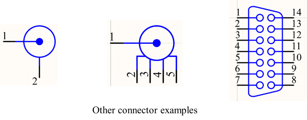
Connectors that are for specific protocols like USB, SATA, JTAG, etc. should have their names visible.
ICs
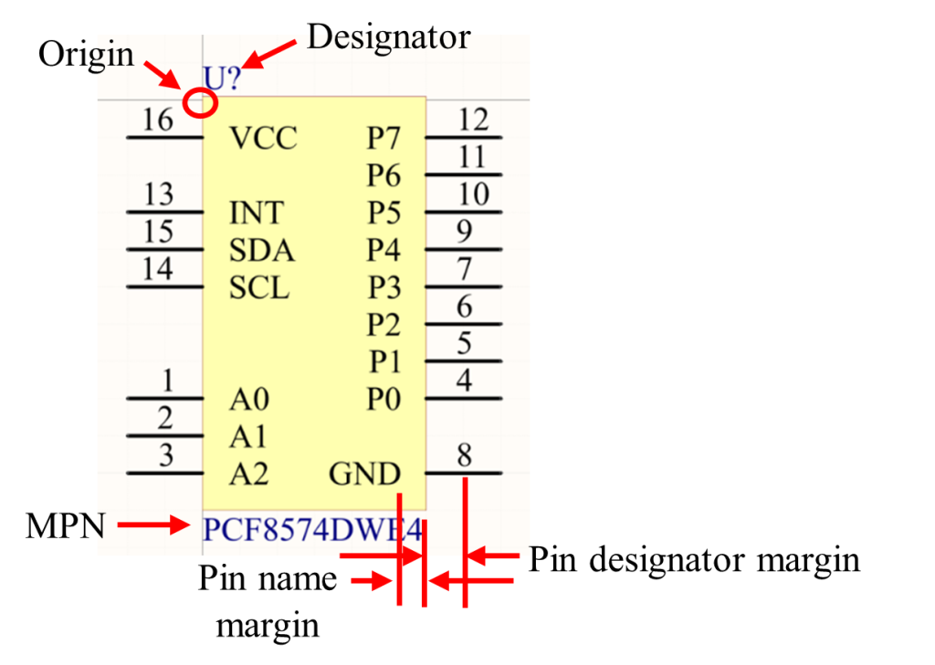
For the purposes of this document, an IC type symbol is one in which the component is represented by a yellow rectangle containing pins that display their numbers and names.
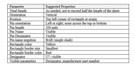
The IC is oriented vertically with the top left corner of the rectangle at the origin. If the symbol is longer than half the paper size, it is broken into multiple symbols, such that none of them are more than half the paper size commonly used by your company. (Paper sizes: A-size - 7500 mils; B-size - 11000 mils; C-size - 17000 mils; A3-size - approximately 11700 mils)
The pins are 200 mils long and both the pin designators (numbers) and the pin names are visible. The width of the rectangle is as big as necessary for all the pin names inside the rectangle to be easily read but not overlapping. The pins are grouped according to function as much as possible, with the inputs on the left side and outputs are on the right side where practical.
Altium allows for pins to be unlocked and moved about in the schematic editor. This allows the user to better organize the connectivity between components. However, other graphics such as the rectangle cannot be modified in the schematic editor. It is suggested that the rectangle be elongated by an extra 200 mils above and below the pins to allow for easier grouping. This is very useful when dealing with microcontrollers and other ICs where the pins may represent multiple functions.
Though the power and ground pins, as shown above, are following a traditional placement flow, an alternative method is to have the power pins on the bottom left and the ground pins on the bottom right. By doing so, bypass caps can be placed and wires with respect to the IC.
